Description
Description
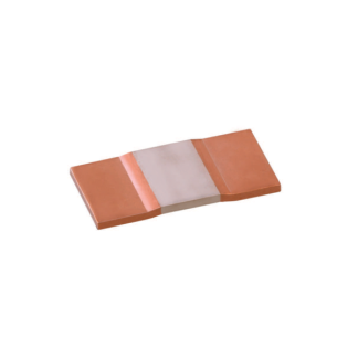
The T Series has the lowest profile of any wire protection grommet edging available.
A steel substrate encapsulated with lubricious fusion bonded nylon gives superior abrasion and chemical resistance.
Key Benefits
- Superior performance: encapsulated stainless steel core: outperforms plastic grommets.
- Snap on installation lowers costs 49% vs. grommets with glue. Watch the 4 min. video below.
- Improves efficiency 9.5x – due to fewer steps in workflow.
Grommet Differentiation Table (GDT)

Applications
- General commercial use to prevent abrasion
- Straight edges
- Small radii inside or outside corners
Features
The old nylon grommet with glue is old, inefficient and costly. DTi has a better way.
- Nylon encapsulated stainless steel substrate
- Snaps on fast with finger pressure
- Installs continuously with two axis conformity, including right angled corners
- Self locking with strong retention – no adhesives
- Simpler install: no adhesive, fixturing, curing, clean up or OSHA concerns
- Maintenance is far easier due to its ease of application, use and removal
- Customization available (lengths, colors and print)
Key Specifications
- Resistant to hydrocarbons, immersion, salt spray, shock and vibration
- Operating Temperature Heat continuous to -40°F to 285°F (-40°C to 140°C)
- UL94 V-0 Flammability Rating
- High Shock and Vibration Resistance to rms G 41.7
- 9 sizes to fit edge thicknesses: 0.02” to 0.26” (0.5 mm to 6.6 mm)
- Factory discrete cut lengths and reels: 25 ft. (7.8 m), 100 ft. (30.5 m), 500 ft. (150 m)
- Tools available: Installation roller, full by-pass shears, castle removal, measuring scale,
go-no go sizing gauge, cutter cart