Description
Overview
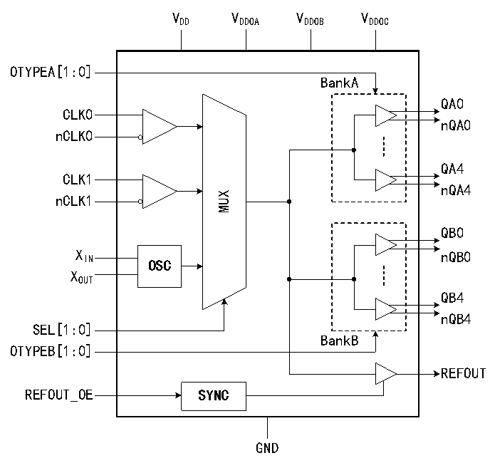
INS6310A is a differential clock buffer with low jitter and low power consumption. The buffer supports one of three clock inputs, ten clock outputs with low jitter differential and one clock output with LVCMOS single-ended. It can flexibly convert the clock level between input and output. The input supports differential, single-ended and passive crystal clock signal.
Product details
• Support 2 sets with 5 differential outputs (LVDS/LVPECL/HCSL/ high-impedance)
• Support 3 inputs
■ 2 differential or single-ended (DC~2500MHz), LVPECL/LVDS/CML/SSTL/HSTL/HCSL
■ 1 passive crystal or single-ended (10M~40MHz)
• Additional phase jitter: 40fs RMS(10KHz~1MHz)
80fs RMS(12KHz~20MHz)
• PSRR: -65/-76dBc(LVDS/LVPECL)@156.25MHz
• Output power: 2.5V/3.3V
• Core supply voltage: 3.3V
• Operation Temperature Range: -40℃~+85℃
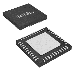
• Package: 7.0*7.0*0.8mm(QFN48)
原理框图
